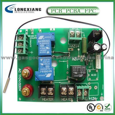
FR4 2-Layer Pcb Assembly
- Application: auto
- OEM No/Model: LX-02
- Market Type:After Market
- FOB Price: USD 1
- Other Price Term: Paypal
- Payment Terms: L/C, D/A, T/T, M/T, D/D, CASH, D/P
- Samples: Not Available
- Minimum Order: 1Piece/Pieces
Quick Details
-
Copper Thickness:
1inch
-
Board Thickness:
1.6mm
-
Min. Hole Size:
0.3mm
-
Min. Line Width:
0.2mm
-
Min. Line Spacing:
0.5mm
-
Surface Finishing:
HASL
- Place of Origin:
China
- Samples:
Not Available
- Delivery Time:
3~5days
- Packing:
Inner:Vacuum Package Outer:Carton
- Delivery Port:
Shenzhen
- Max. Production Capacity:
200000Square Meters Per Month
- Export Ratio:
71% - 80%
- OE Experience:
No
Product Name:FR4 2-Layer Pcb Assembly
FR4 2-Layer Pcb Assembly
Application
auto
Product Description:
OEM No/Model: LX-02
Welcome To Shenzhen Longxiang Intellectual Techonology Co., Ltd.
One-stop service:
- Engineering Services
- PCB layout Design & Assembly
- Product Design
- Prototyping
- Cable and Wire Assemblies
- Plastics and Molds
1.Detailed Specification of PCB Manufacturing
|
1 |
Layer | 1-30 layer |
| 2 | Material | FR-4,CEM-1,CEM-3,Hight TG,FR4 Halogen Free |
| 3 | Board thickness | 0.2mm-6.0mm |
| 4 | Max.finished board side |
550mm*1100mm(single-sided) 550mm*640mm(multilayer) |
| 5 | Min.drilled hole size | 0.15mm |
| 6 | Min.line width | 0.076mm(3mil) |
| 7 | Min.line spaceing | 0.076mm(3mil) |
| 8 | Surface finish/treatment | HALS/HALS lead free,Chemical tin,Chemical Gold,Immersion gold Inmersion Silver/Gold,Osp,Gold Plating |
| 9 | Copper thickness | 0.5-4.0oz |
| 10 | Solder mask color | green/black/white/red/blue/yellow |
| 11 | Inner packing | Vacuum packing,Plastic bag |
| 12 | Outer packing | Standard carton packing |
| 13 | Hole tolerance | PTH:±0.076,NTPH:±0.05 |
| 14 | Certificate | UL,ISO9001,ISO14001,ROHS,CQC |
| 15 | Profiling Punching | Routing,V-CUT,Beveling |
| 16 | Assembly Service | Providing OEM service to all sorts of printed circuit board assembly |
2.Detailed Terms for Pcb Assembly
Technical requirement:
1) Professional Surface-mounting and Through-hole soldering Technology
2) Various sizes like 1206,0805,0603 components SMT technology
3) ICT(In Circuit Test),FCT(Functional Circuit Test) technology.
4) PCB Assembly With UL,CE,FCC,Rohs Approval
5) Nitrogen gas reflow soldering technology for SMT.
6) High Standard SMT&Solder Assembly Line
7) High density interconnected board placement technology capacity.
Quote requirement:
1)Gerber file and Bom list
2)Clear pictures of pcb/ fpc/ pcba or pcba sample for us
3)The PCB specification: Copper thickness(18um or 35um?); Finished board thickness(0.8mm or 1.6mm?); Surface treatment(lead-free HASL or immersion gold?)
4)Test method for PCB/PCBAPCB Layout
Your supply the schematics, we will draw the gerber file then finish the Printed Circuit Board. Our engineers
can also conduct thorough reviews of your existing design and often recommend cost-saving suggestions,
based on proto-type or full run requirements.
PCB Manufacturing Service
· Double-sided, Multi-layer Printed Circuit Boards
· Prototype, Pre-production and Medium to High Volume Production.
· 24 Hours Rush Delivery
· Electrical Testing
Surface Mount Assembly
We offers surface mount technology (SMT) assembly services from proto-type through medium and high
volume production, including fine pitch component. Surface mount capabilities include:
· Semiautomatic Screen Printing
· Place Component upto 19 mil Pitch
· Prototype, Medium to High Volume Production Assembly
· FR4, Aluminum, PI
· Single and Double Sided Assembly
· Mixed Technology(Tjrough Hole & SMT)
· ESD Controlled Area
Through Hole Assembly
PCB Assembly provides through hole or mixed technology assembly solutions. Wave soldering is accomplished
with the latest sophisticated equipment. Our Through hole assembly capabilities include:
· Full Through-Hole Assembly Line
· Prototype, Medium to High Volume Production Assembly
· ESD Controlled Area
Reverse Engineering of Electronic Products
We has developed capabilities of generating the necessary manufacturing documentation from finished
products. Services include:
· Artwork and PCB Scanning
· Schematics and Gerber File Generation
· Bill of Material and Parts List Generation
According to the modelsView More
Supplier Details
You May Like:
-
Electronic Pcb Design China Pcba Supplier
Application: auto
-
SMT Factory China Pcba Manufacturer
Application: auto
-
FR4 Pcba Multilayer Pcb Smt Factory
Application: auto
OEM No: LX-03
-
VOLVO Mercedes Truck Micro Meter Motors XC5 589,XB ...
Application: VOLVO RENAULT ME ...
OEM No: XC5 589 ...
-
Wingle Haval GW2.8TC Bosch Computer Board
Application: Great wall
-
Universal Tacho V2008 Cpu PCB(upgrade)
Application: Bmw/ 3 Series(ch ...
-
HALs Printed Circuit Gold High-frequency Board
Application: Unversal
-
Printed Circuit Board for Audi
Application: Audi/ A6l(china) ...
-
Printed Board FR4 Pcb
Application: None
Related Product Tags:
automotive pcb , Printed Circuit Board PCB , pcb assembly , pcba pcb fpc , mutlilayer pcb , electric iron pcb , PCB , printed circuit board , printed circuit boards , china pcb manufacturer , multilayer pcb , Multilayer Pcb Printed Circuit Board , Osp Printed Circuit Board , Pcb Printed Circuit Board Didn't find what you are looking for?
Please send us Your Search Requirement, or you can Post a Buying Lead,
suppliers may contact you actively.
Please send us Your Search Requirement, or you can Post a Buying Lead,
suppliers may contact you actively.


